-
The buffer is a single-channel (mono) buffer, with the following features:
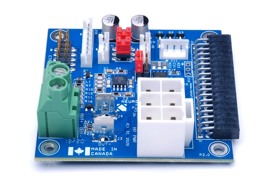
- Differential (balanced, XLR) input, which can easily be configured for single-ended (unbalanced, RCA) operation as well.
- True differential output with common-mode feedback, which ensures a differential output, even when used with a single-ended source.
- Jumper-selectable gain: 0 dB and 13.2 dB for a total amplifier gain of 12.8 dB and 26.0 dB, respectively, when used with the Purifi 1ET400A.
- Gain can be further customized by adding a resistor (1206 size SMD and leaded/PTH supported).
- Plug-and-play connection with Hypex SMPS1200 and future Purifi power supply.
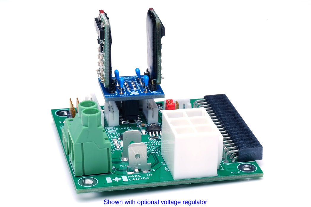
- Opamp power supply: Use the AUX supply provided by the SMPS1200, or add your own regulator. A small daughterboard with support for the Hypex HPR/HNR, LM7812/LM7912, and LM78L12/LM79L12 is available as a product option.
- Status indicator LED output (NC500: CLIP and READY; 1ET400A: READY).
- Speaker output is provided both on 6.3 × 0.81 mm quick-connect spades and a terminal block accepting up to AWG 10 (5.2 mm2) in size.
In addition, the following options are provided for advanced users:
- The buffer can be disabled by removing two resistors. A three-pin connector footprint provides direct access to the Purifi 1ET400A, 1ET6525SA, and Hypex NC500 input.
- A two-pin connector footprint provides access to the remote sensing pins of the Purifi 1ET400A and Hypex NC500.
Please refer to the Purifi 1ET400A, 1ET6525SA, and Hypex NC500 data sheets for further information on how to use these two advanced features.
The Purifi 1ET400A, 1ET6525SA, & Hypex NC500 Input Buffer circuit board is fully assembled, RoHS compliant, and is designed and manufactured in Canada.
-
The full specifications for the Purifi 1ET400A, 1ET6525SA, & Hypex NC500 Input Buffer are tabulated below.
| Parameter |
Value |
Notes |
Quiescent Power Supply Current
|
20 mA
27 mA |
Nominal
Maximum |
| THD |
TBD
(TBD dB) |
Vin = 2.0 V RMS |
| THD+N |
< 0.00025 %
(< -112 dB) |
Vin = 2.0 V RMS |
| THD+N |
0.00025 %
(< -112 dB) |
Vout = 9.6 V RMS |
| IMD: SMPTE 60 Hz + 7 kHz @ 4:1 |
-107 dB
|
Vin = 2.0 V RMS
|
| IMD: DFD 18 kHz + 19 kHz @ 1:1 |
-116 dB
|
Vin = 2.0 V RMS
|
| IMD: DFD 917 Hz + 5.5 kHz @ 1:1 |
-111 dB
|
Vin = 200 mV RMS
|
| Multi-Tone IMD Residual |
< -146 dB Ref.: 9.12 V RMS |
AP 32-tone, Vin = 2.0 V RMS
|
| Gain |
0 dB (1.0×)
13.2 dB (4.8×) |
Can be further customized by resistor option. |
| Gain Flatness |
±0.02 dB |
20 Hz - 20 kHz |
| Bandwidth |
DC – 385 kHz |
100 mV RMS, -3 dB |
| Slew Rate |
±20 V/µs |
Fully symmetric
|
| Common-Mode Rejection Ratio (CMRR) |
> 100 dB
> 65 dB
|
60 Hz, typical
20 kHz, typical
|
| Total Integrated Noise and Residual Mains Hum |
4.0 µV RMS (13 dB)
1.6 µV RMS (0 dB)
|
20 Hz - 20 kHz, A-weighted |
| Total Integrated Noise and Residual Mains Hum |
5.0 µV RMS (13 dB)
2.0 µV RMS (0 dB)
|
20 Hz - 20 kHz, Unweighted |
| Dynamic Range (AES17) |
127 dB |
1 kHz, Vin = 3.1 V RMS |
| Input Impedance |
48 kΩ |
|
| PCB footprint |
64 × 64 mm |
|
| Full module dimensions |
64 × 66 × 28 mm
40 g
|
(W × D × H)
|
All parameters are measured at an opamp power supply voltage of ±12 V, 4.4 kΩ differential (2.2 kΩ from signal to ground) load impedance, differential input, and 13.2 dB gain unless otherwise noted.
Sound Quality
I designed the Purifi 1ET400A / Hypex NC500 Input Buffer to be sonically transparent and firmly believe I have achieved that goal. I generally prefer precise amplifiers as they render the source material naturally, without any colouration, and offer a spacious and realistic sound stage. This aligns well with the design philosophy of Purifi and Hypex as well.
-
The Purifi 1ET400A / Hypex NC500 Input Buffer features a balanced differential input. This input can accept both differential (balanced) signals and, with a simple wire link, single-ended (unbalanced) signals. The Buffer provides a balanced differential output for the Class D amplifier module. The Buffer supports two gain settings, selectable by a jumper: 0 dB and +13.2 dB. This allows for an input-to-output amplifier gain of 26.0 dB when used with the Purifi 1ET400A. The gain of the Buffer can also be customized by adding a resistor (1206 SMD size or leaded/PTH).
The speaker output of the Purifi 1ET400A / Hypex NC500 is brought out on ¼" (6.3 × 0.81 mm) quick-connect spades and on a terminal block supporting the use of speaker wires up to AWG 10 (5.2 mm2) in size.
In addition to the audio signals, the Buffer also provides the CLIP and READY status outputs with appropriate LED drivers. Note that only the Hypex NC500 provides the CLIP signal, whereas both the Purifi 1ET400A and the Hypex NC500 provide the READY signal.
A simplified block diagram of the Purifi 1ET400A / Hypex NC500 Input Buffer is shown below.

-
Measuring the THD of the Purifi 1ET400A / Hypex NC500 Input Buffer is a significant challenge, in particular as the analyzer section of the Audio Precision APx525 analyzer is only good to -125 dB and its source to -112 dB. I normally use a precision oscillator and notch filter for this, but I do not yet have differential versions of these circuits. I will add the FFT plot here once it becomes available. I expect the THD of the Input Buffer to be around -130 dBc at 13.2 dB gain and below -140 dBc at unity gain.
The graph below shows the THD+N vs output level for the two gain settings of the Buffer. The Input Buffer delivers just over +25 dBu (differential) at the onset of clipping, which results in 3.2 dB headroom when used with the Purifi 1ET400A. The difference in THD+N between the two gain settings is caused by the amplification of the APx525 signal source's noise floor. Note that the sharp jumps (aside from when the buffer clips) are caused by range switching in the APx525. The THD+N vs output power plots mostly show the THD+N floor of the measurement system.

As noted, the difference in THD+N between the two gain settings is caused by the buffer amplifying the noise of the signal source in the APx525. You can easily convince yourself of this by examining the plot below, which shows the THD+N vs input level.

Observant readers will note that the input impedance of the Hypex NC500 is lower than that of the Purifi 1ET400A (3.6 kΩ vs 4.4 kΩ, differential, respectively). Thus, I measured the THD+N vs Output Level for the two different impedances. The results are basically line-on-line as shown below.

The THD+N versus frequency measurement below basically shows the noise floor of my APx525 audio analyzer.

Siegfried Linkwitz argues that the 1 kHz + 5.5 kHz intermodulation distortion (IMD) measurement is one of the measurements which is more indicative of the perceived sound quality. He bases this argument on the fact that IMD products in this measurement fall in the frequency range where the ear is the most sensitive (see the Fletcher-Munson curves for more detail). I think this argument carries a good amount of weight, so I measured the Input Buffer accordingly. The measurement is shown below. Note that due to a limitation in the IMD source of the APx525, the frequencies used must be an integer multiple of each other. Thus, I measured at 917 Hz (5500/6) + 5.5 kHz. The result is shown below.

The more conventional IMD measurements are shown below. The two plots show the SMPTE (60 Hz + 7 kHz @ 4:1) IMD and DFD (18 kHz + 19 kHz @ 1:1) IMD, respectively. Poor SMPTE IMD is often indicative of thermal issues or power supply issues in a circuit. The 18k+19k IMD is indicative of the loop gain available in the buffer near the end of the audible spectrum, which can be telling of the sound quality. The Input Buffer provides exemplary performance on both of these measurements.


Audio Precision has developed a multi-tone test signal, which contains 32 tones from 15 Hz to 20 kHz, logarithmically spaced in frequency. This test signal sounds a bit like an out-of-tune pipe organ. It is basically the closest I can get to music with a deterministic test signal. Thus, I argue that this multi-tone signal should be used in an IMD test for the best correlation between measurements and perceived sound quality. I run this test at 2.0 V RMS (which is also the 0 dB reference in the plot). Note that even the tallest IMD components are more than 147 dB below line level. This is likely why the Input Buffer sounds transparent. This measurement shows that it does not add anything (or at least extremely little) to the source signal. Also note that the output is completely free of mains-related hum or noise.

The plot below shows the residual mains hum and noise of the Input Buffer when powered by a regulated power supply. The result shows the buffer outputs only minimal mains-related signal components (which are most likely from the test setup).

The common-mode rejection ratio (CMRR) describes a differential input's ability to reject common-mode signals, such as mains hum. The CMRR of the Purifi/Hypex Input Buffer is shown below.

For completeness, the amplitude response and gain variation are shown below.


Transient Response Measurements
The transient response of the Purifi 1ET400A / Hypex NC500 Input Buffer is shown below. As shown, the response is clean and completely free of ringing and overshoot.


