Measuring the -140 dB THD of the Universal Buffer is a significant challenge, in particular as the analyzer section of the Audio Precision APx525 analyzer is only good to -125 dB and its source to -112 dB. Thus, I use a precision oscillator with a THD below -140 dB and a notch filter to attenuate the fundamental frequency. The resulting measurement of the distortion residual is shown below. As shown, the third harmonic is just below -140 dB at 2 V RMS output voltage.

The graph below shows the THD+N vs output level. The Universal Buffer delivers just over +27 dBu (differential) at the onset of clipping. With single-ended input, the maximum clean output is 6 dB lower. Note that the sharp jumps (aside from when the buffer clips) are caused by range switching in the APx525. The THD+N vs output power plots mostly show the THD+N floor of the measurement system.

The Universal Buffer can be operated at a power supply voltage of ±2.5 to ±17 V. The absolute maximum supply voltage is ±18 V. The power supply should be regulated for the best performance.
Naturally, the maximum clean output voltage provided by the Universal Buffer depends on the applied supply voltage. The relationship is shown in the graph below.

The THD+N versus frequency measurement below basically shows the noise floor of my APx525 audio analyzer.

Siegfried Linkwitz argues that the 1 kHz + 5.5 kHz intermodulation distortion (IMD) measurement is one of the measurements which is more indicative of the perceived sound quality. He bases this argument on the fact that IMD products in this measurement fall in the frequency range where the ear is the most sensitive (see the Fletcher-Munson curves for more detail). I think this argument carries a good amount of weight, so I measured the Universal Buffer accordingly. The measurement is shown below. Note that due to a limitation in the IMD source of the APx525, the frequencies used must be an integer multiple of each other. Thus, I measured at 917 Hz (5500/6) + 5.5 kHz. The result is shown below.

The more conventional IMD measurements are shown below. The two plots show the SMPTE (60 Hz + 7 kHz @ 4:1) IMD and DFD (18 kHz + 19 kHz @ 1:1) IMD, respectively. Poor SMPTE IMD is often indicative of thermal issues or power supply issues in a circuit. The 18k+19k IMD is indicative of the loop gain available in the buffer near the end of the audible spectrum, which can be telling of the sound quality. The Universal Buffer provides exemplary performance on both of these measurements.


Audio Precision has developed a multi-tone test signal, which contains 32 tones from 15 Hz to 20 kHz, logarithmically spaced in frequency. This test signal sounds a bit like an out-of-tune pipe organ. It is basically the closest I can get to music with a deterministic test signal. Thus, I argue that this multi-tone signal should be used in an IMD test for the best correlation between measurements and perceived sound quality. I run this test at 2.0 V RMS (which is also the 0 dB reference in the plot). Note that even the tallest IMD components are more than 147 dB below line level. This is likely why the Universal Buffer sounds transparent. This measurement shows that it does not add anything (or at least extremely little) to the source signal. Also note that the output is completely free of mains-related hum or noise.

The plot below shows the residual mains hum and noise of the Universal Buffer when powered by a regulated power supply. The result shows the buffer outputs only minimal mains-related signal components (which are most likely from the test setup).

As the Universal Buffer is a stereo circuit, I measured the channel separation. As shown below, the channel separation is truly exemplary, measuring nearly 140 dB midband.

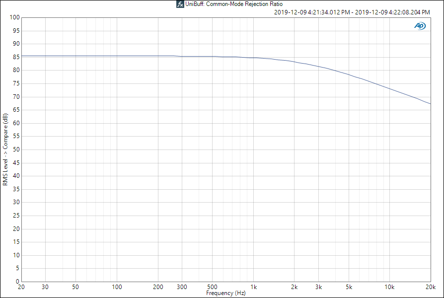
When used with a differential source, the Universal Buffer provides rejection of any signals imposed equally on both wires in the differential signal pair. Common sources of such common-mode noise includes mains hum. As shown below, the Universal Buffer provides more than 85 dB of CMRR at the mains frequency.

For completeness, the amplitude response and gain variation are shown below.


Transient Response Measurements
One of the many applications of the Universal Buffer is as the output stage in a preamplifier. Thus, the Universal Buffer should be able to drive the capacitance of the interconnect cable connecting the Universal Buffer to the power amp or load. This cable capacitance tends to measure roughly 33-50 pF/m. Thus, as shown below, the Universal Buffer is capable of driving over 100 m of interconnect cable cleanly.
The measurements below show the transient response of the Universal Buffer for increasing load capacitance. On its single-ended output, the Universal Buffer drives 10 nF cleanly and 22 nF with controlled overshoot. Even at higher load capacitances, the Universal Buffer remains stable.


The measurements for the differential output are shown below. As shown, the Universal Buffer can drive 4.7 nF cleanly on the differential output and even drive 10 nF with controlled overshoot.


